11. Data calibration Calibration
With the roughly \(\SI{3500}{h}\) of data recorded at CAST it is time to discuss the final calibrations 1 necessary for the calculation of a physics result. On the side of the Septemboard detector this means the 'energy calibration', sec. 11.1; the calculation of the energy of each event recorded with the Septemboard detector. This necessarily needs to include a discussion of detector variability both due to external factors as well as differing detector calibrations and setups, sec. 11.2. Here we provide the reasoning for the choices leading to the final energy calibration, presented in sec. 11.3. Similarly, for the FADC the impact of the noise seen during data taking and resulting differing amplifier settings will be discussed in sec. 11.4.
11.1. Energy calibration - in principle
The reconstructed data from the GridPixes, as described in chapter
9.4 (cluster finding, cluster reconstruction
and charge calibration), still needs to be calibrated in energy. The
charge calibration 8.1.1 computes
the number of electrons recorded on each GridPix pixel in an event
from the ToT counts.
In order to calculate an equivalent energy based on a certain amount
of charge – which depends on the gas gain – the data recorded using
the \cefe calibration source at CAST is used. As the \cefe spectrum
(see sec. 6.3.8) has a photopeak at
\(\SI{5.9}{keV}\) and an escape peak at \(\SI{2.9}{keV}\) it provides two
different lines relating charges to energies for calibration. While
the charge calibration for each pixel from ToT to electrons is
non-linear, the relation between energy and recorded charge is
linear. The position of the two peaks in the \cefe spectrum needs to
be determined precisely, which is done using a double gaussian fit
where \(G\) is a regular gaussian, one for the escape peak \(G^{\text{esc}}\) and one for the photopeak \(G\). An example spectrum with such a fit can be seen in fig. 1(a).


Then, a linear function without y-offset
\[ Q(E) = m_c · E \]
is fitted to the found peak positions of the spectra by charge \(Q\), against the known energies \(E\) of the peaks in the \cefe spectrum. This yields the calibration factor, \(a = m_c⁻¹\), which can be used to calibrate all events with the same gas gain. Over the time of data taking at CAST the gas gain varies by a significant margin, requiring a more complex calibration routine as the calibration factor would produce too imprecise energy values otherwise (for example if each \cefe calibration run were used to deduce one calibration factor \(a = m_c⁻¹\) to be applied to the closest background data in time). An example for this fit is seen in fig. 1(b).
Fortunately, the gas gain can be computed using raw data without evaluating any physical events, allowing calculation of it also for raw background data. This motivates the idea to map a gas gain to a calibration factor needed to calibrate events at such gas gains in energy. Taking a certain time interval in which the detector gas gain is assumed constant, the gas gain of all time slices of this length is computed for background and calibration data. For all time slices in the calibration data the procedure above – fitting the \cefe spectrum and calculating the energy calibration – is performed. A higher gas gain leads to linearly more recorded electrons in the \cefe spectra. Therefore, all energy calibration factors determined from different time intervals should be on a slope depending on the gas gain. As such a final fit
\begin{equation} \label{eq:gas_gain_vs_calib_factor} a(G) = m_g · G + b \end{equation}is performed to all time intervals of all calibration runs. This yields the energy calibration factor \(a\) valid for a given gas gain \(G\). Then in order to calibrate the energy of a given cluster in the background data, the same time slicing is performed and one gas gain calculated for each slice. The gas gain is inserted into the fit and the resulting calibration factor is used to calibrate the energy of every cluster in that time slice. We will come back to this fit in sec. 11.3 to finalize the energy calibration.
The remaining question is the stability of the gas gain over time, which we will look at next in the context of the general detector behavior over time. This allows us to find a suitable time interval to use for all data and hence perform a temporally stable energy calibration.
11.1.1. Generate example plot for \cefe spectrum extended
We use run number 149 (for no important reason) as an example calibration run.
Desktop:
  raw_data_manipulation \
    -p /mnt/4TB/CAST/Data/2018/CalibrationRuns/Run_149_180219-17-25.tar.gz \
    -r calib \
    -o /tmp/run_149.h5
Laptop:
  raw_data_manipulation \
    -p /mnt/1TB/CAST/2018/CalibrationRuns/Run_149_180219-17-25.tar.gz \
    -r calib \
    -o /tmp/run_149.h5
We overwrite the default to use TikZ output via an environment
variable here just to make sure it is set independent of the
config.toml file.
reconstruction -i /tmp/run_149.h5 --out /tmp/reco_149.h5 --useTeX=true --plotOutPath ~/phd/Figs/energyCalibration/run_149/
This produces the following plots:


11.1.2. On ToT vs. ToA for a Timepix1 detector extended
This is a good point to comment on the choice of using all pixels in
the CAST data taking to record ToT values. One might argue that due
to the single electron efficiency of GridPix detectors it would have
been a good idea to either just record only ToA values for all
pixels as to have access to time information (yielding longitudinal
information about events) or at least use a checkerboard pattern with
half the pixels recording ToT and half ToA values.
There are two major issues with that (outside of the fact that at the time of making these choices I was not in a position to make an educated choice anyway):
- the
ToAcounter, as far as I'm aware, is too short for the Timepix1 as needed in the context for CAST like shutter times. Ref (Lupberger 2016) page 30, but the gist is that Timepix1 pixels can count to 11810. At a clock frequency of \(\SI{40}{MHz}\) this only yields a time window of \(\SI{295}{μs}\) forToAvalues. For shutter lengths on the order of seconds such shortToAcounters would run over pretty much always. - ignoring the practical limitation of 1, which may or may not be possible to circumvent in some way or another, there is a separate problem: Single electron efficiency is an ideal approximation of reality. Either for higher energies or in rare cases – which are extremely important for low rate experiments like CAST where "rare" means precisely important for the selection of candidates! – conversion of photons can happen very close to the grid. In those cases many primary electrons will enter single holes, resulting in events with very few pixels but very high charges. See sec. 11.1.2.1 below.
Fortunately, we do have the FADC signal to get at least some time information regardless of the choice.
At the same time in the future with a Timepix3 based GridPix detector
all these points will become mute: it records both ToT and ToA at
the same time at time high resolution. This also means using an FADC
will become irrelevant, avoiding the difficulties of dealing with
analogue signals and associated EMI issues.
11.1.2.1. (While generating fake data) Events with large energy, but few pixels
This section is taken out of my regular notes. It was written while trying to understand certain behaviors while trying to generate fake event data from existing data by removal of pixels. That approach is the easiest way to generate lower energy 'simulated' data from existing data without having to simulate full events (which we ended up doing later anyway).
While developing some fake data using existing events in the photo peak & filtering out pixels to end up at ~3 keV, I noticed the prevalence of events with <150 pixels & ~6 keV energy.
Code produced by splicing in the following code into the body of generateFakeData.
      for i in 0 ..< xs.len:
      if xs[i].len < 150 and energyInput[i] > 5.5:
        #   recompute from data
        let pp = toSeq(  0 ..< xs[i].len  ).mapIt(  (x: xs[i][it], y: ys[i][it], ch: ts[i][it]  )  )
        let newEnergy = h5f.computeEnergy(pp, group, a, b, c, t, bL, mL)
        echo "Length ", xs[i].len , " w/ energy ", energyInput[i], " recomp ", newEnergy
        let df = toDf(  {  "x" : pp.mapIt(it.x.int  ), "y" : pp.mapIt(it.y.int  ), "ch" : pp.mapIt(it.ch.int  )  }  )
        ggplot(df, aes(  "x", "y", color = "ch"  )  ) +
          geom_point() +
          ggtitle(  "funny its real"  ) +
          ggsave(  "/tmp/fake_event.pdf"  )
        sleep(  200  )
    if true: quit  ()
This gives about 100 events that fit the criteria out of a total of O(20000). A ratio of 1/200 seems probably reasonable for absorption of X-rays at 5.9 keV.
While plotting them I noticed that they all share that they are
incredibly dense, like:
![]()
These events must be events where the X-ray to photoelectron conversion happens very close to the grid! This is one argument "in favor" of using ToT instead of ToA on the Timepix1 and more importantly a good reason to keep using the ToT values instead of pure pixel counting for at least some events!
[ ]We should look at number of pixels vs. energy as a scatter plot to see
what this gives us.
11.1.2.2. Plotting low count / high energy events with plotData
Alternatively to the above section we can also just use plotData to
create some event displays for such events for us. We can utilize the
--cuts argument to create event displays only for events with fewer
than a certain number of pixels and more than some amount of energy.
Let's say < 100 pixels and > 5 keV for example:
  plotData \
    --h5file ~/CastData/data/DataRuns2018_Reco.h5 \
    --runType=rtBackground \
    --eventDisplay --septemboard \
    --cuts '("hits", 0, 100)' \
    --cuts '("energyFromCharge", 5.0, Inf)' \
    --cuts '("centerX", 3.0, 11.0)' \
    --cuts '("centerY", 3.0, 11.0)' \
    --applyAllCuts
Or we can produce a scatter plot of how the number of hits relates to
the energy if we make some similar cuts (producing the plot for all
background data obviously drowns it in uninteresting events). We do
this by utilizing the custom --x and --y argument:
  plotData \
  --h5file ~/CastData/data/DataRuns2018_Reco.h5 \
  --runType=rtBackground \
  --x energyFromCharge --y hits --z length \
  --cuts '("hits", 0, 150)' \
  --cuts '("energyFromCharge", 4.0, Inf)' \
  --cuts '("centerX", 3.0, 11.0)' \
  --cuts '("centerY", 3.0, 11.0)' \
  --applyAllCuts
In addition we colored each point by the length of the cluster to see if these clusters are commonly small.
This yields the following plot, fig. 2.

11.2. Detector behavior over time
Outside the detector related issues discussed in section 10.5 the detector generally ran very stable during Run-2 and Run-3 at CAST. This allows and requires to assess the data quality in more nuanced ways. Specifically, the stability of the recorded signals over time is of interest, which is one of the main purposes of the \cefe calibration runs. A fixed spectrum allows to verify stable operation easily. In particular of interest for the energy calibration of the data are the detected charge and gas gain of the detector.
As the charge and gas gain can be computed purely from individual pixel data without any physical interpretation, it serves as a great reference over time. Longer time scale variations of the gas gain were already evident from the calibration runs during data taking and partially expected due to the power supply and grounding problems encountered, as well as different sets of calibrations between Run-2 and Run-3. By binning the data into short intervals of order one hour, significant fluctuations can be observed even on such time scales. Fig. 3 shows the normalized median of the total charge in events for all CAST data normalized by the datasets (background and calibration). Each data point represents a \(\SI{90}{min}\) time slice. Some data is removed prior to calculation of the median as mentioned in the caption. The important takeaway of the figure is the extreme variability of the median charge (up to \(\SI{30}{\%}\)!). Fortunately though, the background and calibration data behaves the same, evident by the strong correlation (purple background, green calibration). While the causes for the variability are not entirely certain (see sec. 11.2.2), it allows us to take action and calibrate the data accordingly.

11.2.1. Generate plot for median of charge over time extended
Let's generate the plot for the median charge within 90 minutes, filtered to only clusters with less than 500 hits, also showing the calibration data, filtered to the silver region & each data type (calibration & background) normalized to 1, as a facet plot.
[X]We handStartHue=285manually here for now, but we should change that to become a thesis wide setting for everything we compile. -> Done.
For a note on why the median and not the mean, see the whole section
on "Detector behavior over time" in the statusAndProgress and in
particular the 'Addendum' there (extreme outliers in some cases is the tl/dr).
  nim c -d:danger -d:StartHue=285 plotTotalChargeOverTime && \
LEFT=4.0 FACET_MARGIN=0.75 ROT_ANGLE=0.0 USE_TEX=true \
         plotTotalChargeOverTime \
         ~/CastData/data/DataRuns2017_Reco.h5 \
         ~/CastData/data/DataRuns2018_Reco.h5 \
         --interval 90 \
         --cutoffCharge 0 \
         --cutoffHits 500 \
         --calibFiles ~/CastData/data/CalibrationRuns2017_Reco.h5 \
         --calibFiles ~/CastData/data/CalibrationRuns2018_Reco.h5 \
         --applyRegionCut \
         --timeSeries \
         --useMedian \
         --normalizeMedian \
         --outpath ~/phd/Figs/behavior_over_time/plotTotalChargeOverTime/ \
         --titleSuff " "
We use a titleSuff suffix of a single space, because a) it's not
empty but b) we don't want an actual suffix (about the cut region etc.).
yielding
among other things, with many more related plots to be found in:
./Figs/behavior_over_time/plotTotalChargeOverTime/
11.2.2. Potential causes for the variability
One possible cause for the variability seen in the previous section is
the electronics of the detector readout. Either a floating ground or
unstable power supply can result in the activation thresholds of the
pixels moving – as was indeed observed – as mentioned in section
10.5. Lesser versions of the problems discussed
in that section could theoretically explain the
variations. Specifically, in regards to the \cefe spectra showing
variation, the number of pixels and the amount of charge are directly
correlated. The number of pixels is plainly a clamped version of the
charge information. If electronics caused threshold variations, it
would both change the effective ToT value as well as the number of
pixels activated in the first place. Fortunately, the center chip also
contains the FADC, which allows for an independent measurement of the
effective charge generated below the grid and thus another indirect
measurement of the gas gain. By comparing how the mean position of the
\cefe spectra behave in the FADC data compared to the GridPix data we
can deduce if the GridPix behavior likely is due to real gas gain
changes or due to electronics.
Fig. 4 shows the (normalized) position of the \cefe photopeak based on a fit to the pixel, charge and FADC spectrum (the latter based on the amplitudes of the FADC signals). Aside from the variations in the FADC data in the 2017 data (left) due to the changed FADC settings (more on that in sec. 11.4), the 'temporally local' changes in all three datasets are almost perfectly correlated. This implies a real physical origin in the observed variation and not an electronic or power supply origin.

A physical change in the gas gain can either be caused by a change in high voltage in the amplification region, a change in gas composition or gas properties (assuming no change in the physical size of the amplification gap, which is reasonable at least within Run-2 and Run-3 as the detector was not touched).
Firstly, the high voltage, while not logged to a file 2, was visually inspected regularly and was always kept at the desired voltages by the Iseg HV module within the operating window. It is a very unlikely source of the variability. 3
Secondly, there is no reason to believe the gas composition to be at fault as a) the detector is used in an open loop at a constant gas flow and b) it would then if anything show up as a sudden change in detector properties upon a gas bottle change and not a continuous change during operation.
This finally leaves the properties of the gas itself, for which three variables are (partially) known:
- the gas flow
- the chamber pressure via the pressure controller on the outlet side
- the temperature
The gas flow was at a relatively constant \(\SI{2}{\liter\per\hour}\). The absolute value should not be too relevant, as the flow is small in absolute terms and thus should have no effect on the gas properties in the chamber as such (via gas flow related effects causing turbulence or similar in the chamber). Its secondary impact is only one on absolute gas pressure, which is controlled by the pressure controller, which provides granular control. While also no log files were written for the chamber pressure, visual inspection was also done regularly and the pressure was at a constant \(\SI{1050}{mbar}\) at most varying by \(\SI{1}{mbar}\) in rare cases, but certainly not in a way correlating to the gas gain variations.
This leaves the temperature inside the chamber and in the
amplification region as the final plausible source of the
variations. As the temperature log files for the Septemboard were lost
due to a software bug (more on that in appendix
sec. 17.2.4), there are two other sources of
temperature information. First of all the shift log of each morning
shift contains one temperature reading of the Septemboard, which
yields one value for every solar tracking. Second of all the CAST slow
control log files contain multiple different temperature readings in
one second intervals. Most notably the ambient temperature in the CAST
hall, which up to an offset (and some variation due to detector load
and cooling efficiency) should be equivalent to the gas
temperature. Fig. 5
shows the normalized temperature sensors in the CAST hall (excluding
the exterior temperature) during the Run-3 data taking period together
with the normalized peak position of the \cefe spectra in pixels
(black points), the temperature from the shift logs (blue points) and
the gas gain values of each chip (smaller points using the color
scale, based on \(\SI{90}{min}\) intervals per point). The blue points
of the temperature of the Septemboard recorded during each solar
tracking nicely follow the temperature trend of the ambient
temperature (T_amb) in the hall, as expected. Comparing the \cefe
spectra mean positions with the shift log temperatures does not allow
to draw meaningful conclusions about possible correlations, due to
lack of statistics. But the gas gains of each chip compared to the
temperature lines does imply an (imperfect) inverse correlation
between the temperature and the gas gain.
As discussed in theory sec. 6.3.6 the expectation for the gas gain given constant pressure is \(G ∝ e^α\) where the first Townsend coefficient \(α\) scales with temperature by
\begin{equation} \label{eq:calib:townsend_scaling_prop} α ∝ \frac{1}{T} \exp\left(-\frac{1}{T}\right). \end{equation}The combination of the inverse relation to \(T\) and its negative exponential is a monotonically increasing sublinear function (and not decreasing as \(1/T\) would imply alone) in the relevant parameter ranges. This should imply an increase in gas gain instead of the apparent decrease we see for increasing temperatures. The kind of scaling according to eq. \eqref{eq:calib:townsend_scaling_prop} was also already experimentally measured for GridPix detectors by L. Scharenberg in (Scharenberg 2019). The implications seem to be that the assumptions going into the \(α\) scaling must have been violated. The septemboard detector in its – essentially open – gas system is a non-trivial thermodynamic system due to the significant heating of the Timepix ASICs and very small amplification region of \(\SI{50}{μm}\) height enclosing a gas mass, where gas flow is potentially inhibited.
This is not meant as a definitive statement about the origins of the gas gain variations in the Septemboard detector data. However, it clearly motivates the need for an even more in depth study of the behavior of these detectors for different gas temperatures at constant pressures (continuing the work of (Scharenberg 2019)). More precise logging of temperatures and pressures in future detectors is highly encouraged. Further, a significantly improved cooling setup (to more closely approach a region where temperature changes have a smaller relative impact), or theoretically even a temperature controlled setup (to avoid temperature changes in the first place) with known inlet gas temperatures might be useful. This behavior is one of the most problematic from a data analysis point of view and thus it should be taken seriously for future endeavors.
See appendix 25 for plots similar to fig. 5 for the other periods of CAST data taking and a scatter plot of the center chip gas gains against the ambient temperature directly.
11.2.2.1. Extended thoughts on missing temperature log data extended
[ ]THINK ABOUT WHETHER TO PUT INTO MAIN AGAIN / REMOVE EXTENDED
Note that even if the temperature logs were still available, it is not obvious how they could lead to a correction that goes beyond the gas gain binning in time that was eventually settled on. The variations lead to gain and loss of information that cannot easily be corrected for without introducing potential biases, especially because the temperature sensor on the bottom side of the Septemboard does not yield an absolute temperature inside the amplification region anyway. While theoretically a fit correlating temperature to energy calibration factors is thinkable it is not clear it would improve the calibration over using gas gains binned in time, as the gas gain is the physical result of temperature changes. The only interesting aspect of it would be potentially higher time resolution than the time binning required to have good statistics for a gas gain. Further, temperature changes are not expected to usually occur on time scales much shorter than of the order of one hour, if they are due to ambient temperature changes. Still, it could be an interesting avenue to explore by experimenting with the available slow control log information on the ambient temperature as a proxy for the temperature in the amplification region (same as the Septemboard temperature sensors, but just with a larger offset and lack of detail regarding local temperature changes due to water cooling related variations).
11.2.2.2. Further thoughts about variability extended
What if (put on my crackpot helmet): At lower temperatures gas diffusion is less efficient. This might lead to stronger effects of "over pressure" / less gas cycling between below and above the grid. This could increase the pressure below the grid as it is further away from an open system in a thermodynamic sense. The higher the temperature the more flow via diffusion exchanges gas below and above the grid, bringing the detector closer to desired 1050 mbar operating window. Yeah right lol.
11.2.2.3. Thoughts about Townsend coefficient & gas gain temperature dependence extended
NOTE: This section was me trying to better understand the origin of the Townsend coefficient and its temperature dependence. The results have since been merged back into the theory part (about mean free path and gas gain) and the main section above.
Some further discussions of the fact that our temperature vs. gain data in fig. 5 seems to imply an inverse proportionality between temperature and gas gain from our data at CAST. So let's go back to our theoretical expectation here and see what we learn.
The number of electrons after a distance \(x\) should be
\[ n = n_0 e^{αx} \]
where \(α\) is the first Townsend coefficient, (Sauli 2014) (eq. 5.2 p. 146). The gas gain is just this divided by the initial number \(n_0\).
Sauli on the definition of the first Townsend coefficient: (Sauli 2014) page 145 eq. 5.1:
The mean free path for ionization λ is defined as the average distance an electron has to travel before having an ionizing collision; its inverse, α = λ⁻¹, is the ionization or first Townsend coefficient, and represents the number of ion pairs produced per unit length of drift; it relates to the ionization cross section through the expression: α = N σi (eq 5.1) where N is the number of molecules per unit volume. As for other quantities in gaseous electronics, the Townsend coefficient is proportional to the gas density and therefore to the pressure P; the ratio α/P is a sole function of the reduced field E/P, as shown in Figure 5.19 for noble gases (Druyvesteyn and Penning, 1940).
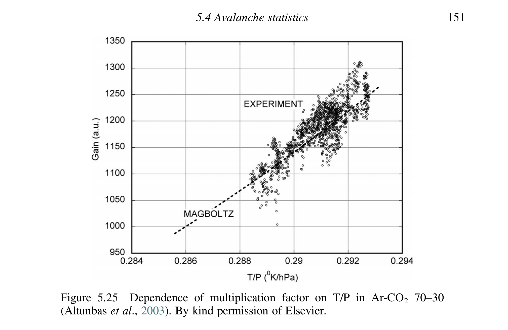
Also from Sauli (Sauli 2014) p. 151 is fig. 6. The plot (data at least) is taken from (Altunbas et al. 2003) and shows a linear (or very shallow exponential) behavior of the gain vs \(T/P\) with experimental data from GEMs for COMPASS and Magboltz simulations as well.
Further papers of interest:
- (Aoyama 1985) -> Contains a mathematical derivation for a generalized first Townsend coefficient relationship with S = E/N (where N is the density and E the electric field).
- (Davydov 2006) contains a discussion about the first Townsend coefficient for very low densities and thus also discussions about the math etc.
Now, if we just go by our intuition from ideal gas physics we would expect the following:
Assuming \(α = 1 / λ\) where \(λ\) is the mean free path. If the temperature increases in a gas, the density decreases for constant pressure \(p\) via
\[ p = ρ R_s T \]
with the specific gas constant \(R_s\). A lower density necessarily implies less particles per unit volume and thus a typically longer path between interactions. This means \(λ\) increases and due to the inverse relationship with \(α\), the first Townsend coefficient – and by extension the gas gain – decreases.
This is even explicitly mentioned by that quote of Sauli above, literally in the sentence
As for other quantities in gaseous electronics, the Townsend coefficient is proportional to the gas density […]
However, this is in stark contrast to
- the screenshot of the fig. above, 6
- the fact that Jochen kept going on about the gas gain being essentially \(G ∝ e^{T/P}\) -> This is clearly wrong, see both below and generally the fact that neither Magboltz nor Lucian's MSc measurements indicate anything of the sorts of an exponential increase with temperature.
- and my Magboltz simulations, sec. 11.2.2.3.2
After a discussion with Lucian today , I'm a little bit more illuminated. In his MSc thesis (Scharenberg 2019) goes through a derivation based on (Engel and Marton 1965) for the temperature dependence of the first Townsend coefficient. Starting from the argument above about \(α = 1/λ\) and then continuing with the requirement to accumulate enough energy to produce secondary ionization events, \(e |\vec{E}| l \geq eV_i\) with the ionization potential \(V_i\) for the gas mixture and \(l\) for the forward distance of an electron under the electric field \(|\vec{E}|\). This distance
\[ l = \frac{V_i}{|\vec{E}|} \]
can be compared to the mean free path \(λ\) of the electron
\[ \mathcal{N} = e^{-l/λ} \]
where \(\mathcal{N}\) is the relative number of colliding electrons with \(l > λ\). This allows to define the probability of finding \(1/l\) collisions per unit distance to be
\[ P(l) \frac{1}{λ} e^{-l / λ} = α \]
which is precisely the definition of the first Townsend coefficient, \(α\).
The mean free path \(λ\) can be related to the pressure \(p\), temperature \(T\) and cross section of the electron in the gas, \(σ\):
\[ λ = \frac{kT}{pσ}. \]
Inserting this into the above definition of \(α\) yields:
\[ α(T) = \frac{pσ}{kT} \exp\left( - \frac{V_i}{|\vec{E}|}\frac{pσ}{kT}\right) \]
which allows to analytically compute the temperature dependence of the first Townsend coefficient, which we'll do in sec. 11.2.2.3.1. The expression now is actually similar to (eq. 5.4) in (Sauli 2014). It seems to roughly match the Magboltz simulations.
Note though that this dependence is 'fragile', as it is a higher order dependence on \(T\) assuming idealized constant parameters for \(p\) and \(σ\) and gas composition. In reality it is easily thinkable that gas contamination and slight variations in pressure can change the results from this result.
- Applying Lucians (eq. 5.17) formula and plotting it
Lucian gives the following formula for the temperature dependence of the first Townsend coefficient:
\[ α(T) = \frac{pσ}{kT} \exp\left( - \frac{V_i}{|\vec{E}|}\frac{pσ}{kT}\right) \]
where \(p\) is the gas pressure, \(σ\) the cross section of electrons with the gas at the relevant energies, \(V_i\) the ionization potential for the gas, \(|\vec{E}|\) the electric field strength.
import unchained, math, ggplotnim, sequtils const V_i = 15.7.V # Lucian gives this ionization potential next to fig. 5.4 defUnit(kV•cm⁻¹) defUnit(cm⁻¹) proc townsend [ P: Pressure; A: Area ](p: P, σ: A, T: Kelvin, E: kV•cm⁻¹): cm⁻¹ = let arg = ( V_i * p * σ) / ( E * k_B * T ) echo arg result = (p * σ / (k_B * T ) * exp( -arg ) ).to(cm⁻¹) echo townsend( 1013.25.mbar, 500.MegaBarn, 273.15.K, 60.kV•cm⁻¹) let temps = linspace( 0.0, 100.0, 1000 ) # 0 to 100 °C # let temps = linspace(-273.15, 10000.0, 1000) # all of da range! var αs = temps.mapIt(townsend( 1013.25.mbar, 500.MegaBarn, ( 273.15 + it).K, 60.kV•cm⁻¹).float ) let df = toDf(temps, αs) ggplot(df, aes( "temps", "αs" ) ) + geom_line() + xlab( "Gas temperature [°C]" ) + ylab( "Townsend coefficient [cm⁻¹]" ) + theme_font_scale( 1.0, family = "serif" ) + ggsave( "~/phd/Figs/gas_physics/townsend_coefficient_temperature_scaling_lucian.pdf" ) - Simulations with Magboltz
I wrote a simple interfacing library with Magboltz for Nim:
https://github.com/SciNim/NimBoltz ./../CastData/ExternCode/NimBoltz/nimboltz.nim
and I ran simulations at different temperatures, but same pressure and the first Townsend coefficient (based on the steady state simulation, which should be the correct one for high fields
The simulation of avalanche gain detectors at high field requires the use of SST Townsend parameters.
from https://magboltz.web.cern.ch/magboltz/usage.html and line 256 in ./../src/Magboltz/magboltz-11.17.f.
These seem to indicate that the coefficient should increase.
Why? -> See above!
11.2.2.4. TODO Note about variability in GridPix 1 extended
[ ]CREATE TEMPERATURE PLOT OF TEMP IN CAST HALL DURING GRIDPIX1 DATA! -> for noexport this is very useful info.
Christoph did see variations in his gas gain as well!! Fig. 9.7 of his thesis and he even notes it is likely due to temperature effects in the hall! The big difference is just that the absolute variations were quite a bit smaller.
Why this has never been on the mind of people like Jochen I will never understand…
Further: in fig. 7.26 he even sees significant differences in the gas gain for different targets of CDL data. But he concludes (by taking a cut) that this is due to multiple electrons in the same hole instead of real changes. Likely a combination of both I assume.
11.2.2.5. Generate plot of \cefe peak position extended
From my zsh history:
  : 1672709064:0;./mapSeptemTempToFePeak ~/CastData/data/CalibrationRuns2017_Reco.h5 --inputs fePixel --inputs feCharge --inputs feFadc
: 1672709066:0;evince /t/time_vs_peak_pos.pdf
: 1672709148:0;cp /t/time_vs_peak_pos.pdf ~/phd/Figs/time_vs_55fe_peak_pos_2017.pdf
First of all we need to make sure our calibration HDF5 file not only has the reconstructed \cefe spectra including their fits, but also the fits for the FADC spectra. If that is not the case:
- Make sure the FADC data is fully reconstructed:
reconstruction -i ~/CastData/data/CalibrationRuns2017_Reco.h5 --only_fadc
- Now redo the \cefe fits:
reconstruction -i ~/CastData/data/CalibrationRuns2017_Reco.h5 --only_fe_spec
With that done we can create a plot of all normalized \cefe peak positions and compare it to the temperatures recovered from the CAST shift forms of the septemboard.
    WRITE_PLOT_CSV=true USE_TEX=true ./mapSeptemTempToFePeak \
#               ~/CastData/data/CalibrationRuns2017_Reco.h5 \
                    /mnt/1TB/CAST/2017/CalibrationRuns2017_Reco.h5 \
             --inputs fePixel --inputs feCharge --inputs feFadc \
             --outpath ~/phd/Figs/behavior_over_time/mapSeptemTempToFePeak/
Note that the plot that we include in the thesis from the following created:


is actually one of the ones that does not include the septemboard temperatures from the shift forms. That's because of the much more in depth plot below of course!
11.2.2.6. Generate plot of ambient CAST temp against 55Fe peaks extended
First we run the CAST log reader to get the temperature data as a
simple CSV file (by default just written to
/tmp/temperatures_cast.csv):
    cd $TPA/LogReader #   <- directory of TimepixAnalysis
./cast_log_reader sc -p ../resources/LogFiles/SClogs -s Version.idx
Note that this requires the slow control files for the relevant times
to be present in the SCLogs directory!
[ ]MOVE CODE OVER TO TPA, DEDUCTION TO STATUS, MAYBE KEEP HERE AS WELL? -> well, the interesting stuff will go straight into the thesis, so there is less
    import std / [strutils, sequtils, times, stats, strformat]
import os except FileInfo
import ggplotnim, nimhdf5
import ingrid / tos_helpers
import ingrid / ingrid_types

type
  FeFileKind = enum
    fePixel, feCharge, feFadc

let UseTex = getEnv(  "USE_TEX", "false"  ).parseBool
let Width = getEnv(  "WIDTH", "1000"  ).parseFloat
let Height = getEnv(  "HEIGHT", "600"  ).parseFloat

const Peak = "μ"
let PeakNorm = if UseTex: r"$μ/μ_{\text{max}}$" else: "μ/μ_max"
const TempPeak = "(μ/T) / max"
let T_amb = if UseTex: r"$T_{\text{amb}}$" else: "T_amb"

proc readFePeaks  (files: seq  [  string  ], feKind: FeFileKind = fePixel): DataFrame =
  const kalphaPix = 10
  const kalphaCharge = 4
  const parPrefix = "p"
  const dateStr = "yyyy-MM-dd'.'HH:mm:ss" #   example: 2017-12-04.13:39:45
  var dset: string
  var kalphaIdx: int
  case feKind
  of fePixel:
    kalphaIdx = kalphaPix
    dset = "FeSpectrum"
  of feCharge:
    kalphaIdx = kalphaCharge
    dset = "FeSpectrumCharge"
  of feFadc:
    kalphaIdx = kalphaCharge
    dset = "FeSpectrumFadcPlot" #   raw dataset is `  minvals  ` instead of `  FeSpectrumFadc  `

  var h5files = files.mapIt(  H5open  (it, "r"  )  )
  var fileInfos = newSeq  [  FileInfo  ]()
  for h5f in mitems  (h5files):
    let fi = h5f.getFileInfo()
    fileInfos.add fi
  var
    peakSeq = newSeq  [  float  ]()
    dateSeq = newSeq  [  float  ]()
  for (h5f, fi) in zip(h5files, fileInfos):
    for r in fi.runs:
      let group = h5f[  (recoBase() & $r).grp_str]
      let chpGrpName = if feKind in {fePixel, feCharge}: group.name / "chip_3"
                       else: group.name / "fadc"
      peakSeq.add h5f[  (chpGrpName / dset).dset_str].attrs[
        parPrefix & $kalphaIdx, float
      ]
      dateSeq.add parseTime(group.attrs[  "dateTime", string  ],
                            dateStr,
                            utc()  ).toUnix.float
  result = toDf(  { Peak : peakSeq,
                  "Timestamp" : dateSeq }  )
    .arrange(  "Timestamp", SortOrder.Ascending  )
    .mutate(f{  float: PeakNorm ~ idx(  Peak  ) / max  (col(  Peak  )  )  },
            f{  "Type" <- $feKind}  )

proc toDf  [  T: object  ](data: seq  [  T  ]  ): DataFrame =
  ## Converts a seq of objects that (may only contain scalar fields) to a DF
  result = newDataFrame()
  for i, d in data:
    for field, val in fieldPairs  (d):
      if field notin result:
        result  [field] = newColumn(toColKind(  type  (val)  ), data.len  )
      result  [field, i] = val

proc readGasGainSliceData  (files: seq  [  string  ]  ): DataFrame =
  result = newDataFrame()
  for f in files:
    let h5f = H5file  (f, "r"  )
    let fInfo = h5f.getFileInfo()
    for r in fInfo.runs:
      for c in fInfo.chips:
        let group = recoDataChipBase(r) & $c
        var gainSlicesDf = h5f[group & "/gasGainSlices90", GasGainIntervalResult  ].toDf
        gainSlicesDf[  "Chip"  ] = c
        gainSlicesDf[  "Run"  ] = r
        gainSlicesDf[  "File"  ] = f
        result.add gainSlicesDf
    discard h5f.close  ()

const periods = [  (  "2017-10-30", "2017-12-23"  ),
                 (  "2018-02-15", "2018-04-22"  ),
                 (  "2018-10-19", "2018-12-21"  )  ]

proc toPeriod  (x: int  ): string =
  let date = x.fromUnix()
  for p in periods:
    let t0 = p[  0  ].parseTime(  "YYYY-MM-dd", utc()  )
    let t1 = p[  1  ].parseTime(  "YYYY-MM-dd", utc()  )
    if date >= t0 and date <= t1: return p[  0  ]

proc mapToPeriod  (df: DataFrame, timeCol: string  ): DataFrame =
  result = df.mutate(f{  int -> string: "RunPeriod" ~ toPeriod(idx(timeCol)  )  }  )
    .filter(f{  string -> bool: `RunPeriod`.len > 0  }  )

proc readSeptemTemps  (): DataFrame =
  const TempFile = "/home/basti/CastData/ExternCode/TimepixAnalysis/resources/cast_2017_2018_temperatures.csv"
  const OrgFormat = "'<'yyyy-MM-dd ddd H:mm'>'"
  result = toDf(readCsv(  TempFile  )  )
    .filter(f{c"Temp / °" != "-"  }  )
  result  [  "Timestamp"  ] = result  [  "Date"  ].toTensor(  string  ).map_inline(parseTime(x, OrgFormat, utc()  ).toUnix)

proc readCastTemps  (): DataFrame =
  result = readCsv(  "/tmp/temperatures_cast.csv"  )
    #  .filter(f{float: `  Time  ` >= t0 and `  Time  ` <= t1})
    .group_by(  "Temperature"  )
    .mutate(f{  "TempNorm" ~ `TempVal` / max  (col(  "TempVal"  )  )  }  )
    .filter(f{`Temperature` != "T_ext"  }  )
  var newKeys = newSeq  [  (  string, string  )  ]()
  if UseTex:
    result = result.mutate(f{  string -> string: "Temperature" ~ (
      let suff = `Temperature`.split(  "_"  )[  1  ]
      r"$T_{\text{" & suff & "}}$"  )
    }  )
    echo "Resulting DF: ", result

proc toPeriod  (v: float  ): string =
  result = v.int.fromUnix.format(  "dd/MM/YYYY"  )

proc keepEvery  (df: DataFrame, num: int  ): DataFrame =
  ## Keeps only every `  num  ` row of the data frame
  result = df
  result  [  "idxMod"  ] = toSeq(  0 ..< df.len  )
  result = result.filter(f{  int -> bool: `idxMod` mod num == 0  }  )

proc plotCorrelationPerPeriod  (df: DataFrame, kind: FeFileKind, gainDf, dfCastTemp, dfTemp: DataFrame,
                              period, outpath = "/tmp"  ) =
  let t0 = df[  "Timestamp", float  ].min
  let t1 = df[  "Timestamp", float  ].max

  let dfCastTemp = dfCastTemp
    .keepEvery(  50  )
    .filter(f{  float: `Time` >= t0 and `Time` <= t1}  )
  let dfTemp = dfTemp
    .filter(f{  float: `Timestamp` >= t0 and `Timestamp` <= t1}  )
  var gainDf = gainDf
    .filter(f{  float: `tStart` >= t0 and `tStart` <= t1}  )
    .mutate(f{  float: "gainNorm" ~ `G` / max  (col(  "G"  )  )  }  )
  echo gainDf

  ## XXX: combine point like data for legend?
  #   let dfC = bind_rows([("Fe55", df), ("SeptemTemp", dfTemp)], "Type")
  var plt = ggplot(df, aes(  "Timestamp", PeakNorm  )  ) +
    geom_line(data = dfCastTemp, aes = aes(  "Time", "TempNorm", color = "Temperature"  )  ) +
    geom_point() +
    scale_x_continuous(labels = toPeriod)

  if dfTemp.len > 0: #   only if septemboard data available in this period
    plt = plt + geom_point(data = dfTemp, aes = aes(  "Timestamp", f{idx(  "Temp / °"  ) / max  (col(  "Temp / °"  )  )  }  ), color = "blue"  )


  block AllChips:
    plt + geom_point(data = gainDf, aes = aes(  "tStart", "gainNorm", color = gradient(  "Chip"  )  ), alpha = 0.7, size = 1.5  ) +
      ggtitle(  "Correlation between temperatures (Septem = blue points) \\& 55Fe position " & $kind &
        " (black) and gas gains by chip", titleFont = font(  11.0  )  ) +
      themeLatex(fWidth = 0.9, textWidth = 677.3971, #   the `  \textheight  `, want to insert in landscape
                  width = Width, height = Height, baseTheme = singlePlot) +
      margin(bottom = 2.5  ) +
      ggsave(&"{outpath}/correlation_{kind}_all_chips_gasgain_period_{period}.pdf",
              width = 1000, height = 600,
              useTeX = UseTeX, standalone = UseTeX  )

  block CenterChip:
    gainDf = gainDf.filter(f{`Chip` == 3  }  )
    plt + geom_point(data = gainDf, aes = aes(  "tStart", "gainNorm"  ), color = "purple", alpha = 0.7, size = 1.5  ) +
      ggtitle(  "Correlation between temperatures (Septem = blue points) \\& 55Fe position " & $kind &
        " (black) and gas gains (chip3) in purple", titleFont = font(  11.0  )  ) +
      themeLatex(fWidth = 0.9, textWidth = 677.3971, #   the `  \textheight  `, want to insert in landscape
                 width = Width, height = Height, baseTheme = singlePlot) +
      ggsave(&"{outpath}/correlation_{kind}_period_{period}.pdf", width = 1000, height = 600,
             useTeX = UseTeX, standalone = UseTeX  )

proc plotCorrelation  (files: seq  [  string  ], kind: FeFileKind, gainDf, dfCastTemp, dfTemp: DataFrame,
                     outpath = "/tmp"  ) =
  let df = readFePeaks(files, feCharge)
    .mapToPeriod(  "Timestamp"  )

  for (tup, subDf) in groups(df.group_by(  "RunPeriod"  )  ):
    plotCorrelationPerPeriod(subDf, kind, gainDf, dfCastTemp, dfTemp, tup[  0  ][  1  ].toStr, outpath)

proc plotTempVsGain  (dfCastTemp, gainDf: DataFrame, outpath: string  ) =
  ## Now let's plot the actual gas gain against the temperature in each slice.
  ## Only for the center chip.
  ## 1. compute mean temperature within time associated with each gain value
  #   dfCastTemp
  #   gainDf
  ## NOTE: We do not compute the mean temperature associated with the
  proc mapGainToTemp  (gainDf, dfCastTemp: DataFrame, period: string  ): DataFrame =
    let t0G = gainDf[  "tStart", int  ].min
    let t1G = gainDf[  "tStop", int  ].max
    #   filter temperature data to relevant range
    echo dfCastTemp.isNil
    echo dfCastTemp
    let dfF = dfCastTemp
       .filter(f{  int: `Time` >= t0G and `Time` <= t1G},
               f{  string -> bool: `Temperature` == T_amb  }  )

    var cT: RunningStat
    let ambT = dfF[  "TempVal", float  ]
    let time = dfF[  "Time", int  ]

    var j = 0
    let gDf = gainDf.filter(f{  int -> bool: `Chip` == 3  }  )
    var temps = newSeq  [  float  ](gDf.len  )
    ## we now walk all temperatures and accumulate them in a `  RunningStat  ` to compute
    ## the mean within `  tStart  ` and `  tStop  ` (by `  tStart  ` of the next slice).
    ## First and last are just copied from ambient temperature values.
    temps[  0  ] = ambT[  0  ]
    for i in 1 ..< gDf.high:
      while time[j] < gDf[  "tStart", int  ][i]:
        cT.push ambT[j]
        inc j
      temps[i] = cT.mean
      cT.clear()
    temps[gDf.high  ] = ambT[ambT.len - 1  ]
    let gains = gDf[  "G", float  ]
    result = toDf(temps, gains, period)

  var dfGT = newDataFrame()
  for (tup, subDf) in groups(gainDf.groupBy(  "RunPeriod"  )  ):
    dfGT.add mapGainToTemp(subDf, dfCastTemp, tup[  0  ][  1  ].toStr)
  echo dfGT
  echo dfGT.tail(  100  )
  ggplot(dfGT.filter(f{`temps` > 0.0  }  ), aes(  "temps", "gains", color = "period"  )  ) +
    geom_point() +
    ggtitle(  "Gas gain (90 min slices) vs ambient T at CAST (center chip)"  ) +
    xlab(  "Temperature [°C]"  ) + ylab(  "Gas gain"  ) +
    themeLatex(fWidth = 0.9, width = 600, baseTheme = singlePlot) +
    ggsave(&"{outpath}/gain_vs_temp_center_chip.pdf",
           width = 600, height = 360,
           useTeX = UseTeX, standalone = UseTeX  )

proc main  (calibFiles: seq  [  string  ], dataFiles: seq  [  string  ] = @[],
          outpath = "/tmp/"  ) =
  ## NOTE: this file needs the CSV file containing the temperature data from the slow control
  ## CAST log files, which is written running the `  cast_log_reader  ` on the slow control log
  ## directory!
  var gainDf = newDataFrame()
  if dataFiles.len > 0:
    gainDf = readGasGainSliceData(dataFiles)
      .mapToPeriod(  "tStart"  )
    ## Make a plot of the raw gas gains of all chips
    ggplot(gainDf, aes(  "tStart", "G", color = "Chip"  )  ) +
      geom_point(size = 2.0  ) +
      ggtitle(  "Raw gas gain values in 90 min bins for all chips"  ) +
      themeLatex(fWidth = 0.9, width = Width, height = Height, baseTheme = singlePlot) +
      ggsave(&"{outpath}/raw_gas_gain.pdf",
             width = 600, height = 360,
             useTeX = UseTeX, standalone = UseTeX  )

  let dfCastTemp = readCastTemps()
  let dfTemp = readSeptemTemps()
  plotTempVsGain(dfCastTemp, gainDf, outpath)

  plotCorrelation(calibFiles, fePixel,  gainDf, dfCastTemp, dfTemp, outpath)
  plotCorrelation(calibFiles, feCharge, gainDf, dfCastTemp, dfTemp, outpath)

when isMainModule:
  import cligen
  dispatch main
Running the above as:
    USE_TEX=true WRITE_PLOT_CSV=true code/correlation_ambient_temps_fe55_peaks \
    ~/CastData/data/CalibrationRuns2017_Reco.h5 \
    ~/CastData/data/CalibrationRuns2018_Reco.h5 \
    -d ~/CastData/data/DataRuns2017_Reco.h5 \
    -d ~/CastData/data/DataRuns2018_Reco.h5 \
    --outpath ~/phd/Figs/behavior_over_time/
which generates the following plots:


of which we insert only one of them (Run 3) correlation of gas gains and temperature against the time. That is mainly because in that period there was no worry about power supply effects anymore. It should be noted that the apparent inverse correlation is not apparent in the Run-2 data of 2017. Generally the water cooling was working better at those times, which may be relevant. I don't want to introduce even more speculation into the main section and as the scatter plot of gas gain and temperature clearly shows an inverse correlation for a large chunk of the data, the existing text is justified.
Also, we chose to include the fePixel version and not the feCharge
version as the link between gas gain of the center chip and the \cefe
charge spectrum is much more direct, offering less additional information.
- Initial interpretation upon seeing the correlation plot
Note: this text was written after I created the first version of the above plot for the first time.
The first thing that jumps out is that the (normalized) temperature recovered from the shift forms of the Septem board sensor is strongly correlated with the ambient CAST temperature (
T_amb). This is interesting and reassuring as it partially explains why the temperatures were higher on the Septemboard during Run-3 than Run-2: it was hotter in the hall in Run-3 (not shown in this plot, see full version of all data).Next paragraph was written before gas gain information was in the plot However, the peak position of the 55Fe data is either uncorrelated or actually inversely proportional to the temperatures. When the temperatures are lower the peak position is higher and vice versa. The data is imo not good enough to make final statements about this, but something might be going on there. This is something that one might want to investigate in the future!
UPDATE: Having added the gas gain slice information to the plot now, it seems pretty evident that there is an inverse correlation between the gas gain and the temperature!
- ideal gas, temp + constant pressure, lower density, higher mobility
- less visible in old detector, as absolute temperatures under grid much lower, therefore on a "less steep" part of the exponential that makes up the gas gain temperature dependence!
PDG 2016 page 467 says: (detectors at accelerators chapter)
For different temperatures and pressures, the mobility can be scaled inversely with the density assuming an ideal gas law
This should imply:
- A higher temperature in the CAST hall, while keeping the same pressure in the detector, means a lower gas density according to the ideal gas law, p·V = nRT ⇔ n₁RT₁ = n₂RT₂ ⇔ T₁/T₂ = n₁/n₂ ⇔ T₁ > T₂ ⇒ n₁ < n₂. n ∝ ρ.
- A lower density according to the quote then implies a higher mobility.
- The 'mobility' should be proportional to the mean free path.
[ ]CHECK THIS
- Assuming the mean free path is long enough in 'both' temperatures as to have enough kinetic energy to cause an ionization ~typically, then a higher mobility means less gas gain, as there will be less collisions! However if the mean free path would lead to typical collisions that do not have enough energy to cause ionization, then the gas gain would be lower for a lower mobility, as the gas would then act as a dampener. But the former should always be true in the amplification region I guess.
This explanation is not meant as a definitive statement about the origins of the gas gain variations in the Septemboard detector data. However, it clearly motivates the need for an in depth study of the behavior of these detectors for different gas temperatures at constant pressures and more precise logging of temperatures in future detectors. Further, a significantly improved cooling setup (to more closely approach a region where temperature changes have a smaller relative impact), or theoretically even a temperature controlled setup with known inlet gas temperatures might be useful. This behavior is one of the most problematic from a data analysis point of view and thus it should be taken seriously for future endeavors!
[X]INSERT THE PIXEL TEMP GASGAIN PLOT INTO THESIS ROTATED FULL PAGE?[X]ADD VERSION OF PLOTS THAT SHOW FULL DATA WITHOUT CUT TO RUN-3[X]ADD A SIMILAR PLOT, BUT NOT USING 55FE POSITIONS, BUT GAS GAIN SLICES -> done by adding Gas gain data as well for all chips!
11.2.3. Gas gain binning
Motivated by the strong variation seen over timescales much shorter than the typical length of a background run, the gas gain needs to be computed in time slices of a fixed length. This is naturally a trade-off between assigning accurate gas gains to a time slice and acquiring enough statistics to compute said gas gain correctly.
To determine a suitable time window the gas gain was computed for a fixed set of different time intervals and figures similar to fig. 3 were considered not only for the median charge, but also different geometric cluster distributions. Further, by applying the energy calibration based on each different set of time intervals to the background data (as will be explained in sec. 11.3), the histograms of the median cluster energy in the background data was studied. The ideal time interval is one in which the resulting median energy distribution has low variance and is unimodal approaching a normal distribution, (background in all slices is equivalent over large enough times) while at the same time provides enough statistics in the \cefe spectrum of the slice to perform a good fit.
Unimodality can be quantitatively checked using different goodness of fit tests (Anderson-Darling, Cramér-von Mises, Kolmogorov-Smirnov). See appendix 25.1 for a comparison and further plots comparing the intervals. The goodness of fit tests tend to favor shorter intervals, in particular \(\SI{45}{min}\). However, looking at fig. 7 shows that the variance grows significantly below \(\SI{90}{min}\).

As the different ways to look at the data are not entirely conclusive, the choice was made to choose an interval length that is not too long, while still providing enough statistics for the \cefe spectra. As such \(\SI{90}{min}\) was selected as the final interval time. Of course no data taking run is a perfect multiple of \(\SI{90}{min}\). The last slice smaller than the time interval is either added to the second to last slice (making it longer than \(\SI{90}{min}\)) if it is smaller than some fixed interval or will be kept as a single shorter interval. This is controlled by an additional parameter that is set to \(\SI{25}{min}\) by default. 4
11.2.3.1. Ridgeline plot of the median energies extended
Finally, let's recreate the plot of the histograms of the median energies in the time slices as a ridgeline plot to better explain why we chose 90 min instead of anything else that we tested.
First, if one is not happy with using the provided CSV files that
contain the precomputed medians of the cluster energy in the
phd/resources/optimize_gas_gain_length directory, run the
optimizeGasGainSliceTime tool:
    cd $TPA/Tools
nim c -d:release -d:StartHue=285 optimizeGasGainSliceTime.nim
./optimizeGasGainSliceTime --path <PathToDataRunsH5> --genCsv
Note that this takes some time, as the fitting of all gas gains in each time slice is somewhat time consuming (for the 90 min case it takes maybe 15 minutes for all data; more for shorter time scales, less for longer). (It may be necessary to modify the code as I may forget to change the input data file paths; they are hardcoded as of right now)
[ ]CHANGE CODE TO NOT USE HARDCODED PATHS, THEN ADJUST SCRIPT ABOVE -> Change code to not point to hardcoded config file!
This generates CSV files in an out directory from wherever you
actually ran the code from.
To produce the plots as used in the thesis (and many more), just run:
    USE_TEX=true WIDTH=600 HEIGHT=380 FACET_MARGIN=1.1 LINE_WIDTH=1.0 WRITE_PLOT_CSV=true \
             ./optimizeGasGainSliceTime \
             --path out \
             --plot \
             --outpath ~/phd/Figs/behavior_over_time/optimizeGasGainSliceTime/
Among others this generates a plot of the scores for different goodness of fit tests for each interval setting and period of data taking. They all use the mean of the full data and the variance of the full data (that's clearly not ideal, but it should be passable to have something comparable).
The resulting plot is
 At least for the 2017 data set the 45 minute interval seems to be the
clear winner. However, in beginning 2018 it's one of the worst at
least for Anderson-Darling and Cramér-von-Mises (which are probably
the most interesting tests to look at).
At least for the 2017 data set the 45 minute interval seems to be the
clear winner. However, in beginning 2018 it's one of the worst at
least for Anderson-Darling and Cramér-von-Mises (which are probably
the most interesting tests to look at).
The 90 min result is sort of mostly in the middle. The big advantage of it though is that it definitely captures enough statistics, which is extremely important for the \cefe spectrum, as the data rate is very low there. As much statistics as possible is needed to get a nice fit there.
At the same time comparing the ridgeline plot / histograms it is also evident that the variance itself is quite a bit smaller in the 90 min case, which is another important aspect.
In addition all these plots for the distribution of properties / the energy are created:


11.3. Energy calibration dependence on the gas gain
With the final choice of time interval for the gas gain binning in
place, the actual calibration used for further analysis can be
presented. Fig. 8
shows the fits according to the linear relation as explained in
sec. 11.1, eq. \eqref{eq:gas_gain_vs_calib_factor}, for the
two data taking campaigns, Run-2 in
8(a) and Run-3 in
8(b). Each point represents one
\(\SI{90}{min}\) slice of calibration data for which a \cefe spectrum
was fitted and then the linear energy calibration performed. The
resulting energy calibration factor is then plotted against the gas
gain computed for this time slice. The uncertainty of each point is
the uncertainty extracted from the fit parameter of the calibration
factor after error propagation. Calibrations need to be performed
separately for each data taking campaign as the detector behavior
changes due to different detector calibrations. These have an impact
on the ToT calibration as well as the activation threshold. Note
that the reduced \(χ²\) values shown in the figure, implies that this
calibration does not perfectly calibrate out the systematic effects of
the variability.


To compare the energy calibration using single gas gain values for each full run against the method of time slicing them to \(\SI{90}{min}\) chunks, we will look at the median cluster energy in each time slice for background and calibration data. This is the same idea as behind fig. 3 previously, just for the energy instead of charge. This yields fig. 9. The points represent background and crosses calibration data. Green is the unbinned (full run) approach and purple the binned approach using \(\SI{90}{min}\) slices. The effect is a slight, but visible reduction in variance. It represents an important aspect of increasing data reliability and lowering associated systematic uncertainties. Note that the variability looks much smaller than in fig. 3 due to not being normalized. However, here we wish to emphasize that the absolute energy calibration yields a flat result and matches our expectation.
As such the final energy calibration works by first deducing the gas gain at the time of an event, computing the calibration factor required for this gas gain and finally using that factor to convert the charge into energy.

11.3.1. Generate plot for the gas gain vs. energy calibration factors extended
In principle the plots shown in the section above are produced during
the regular data reconstruction and calibration, in particular by the
reconstruction program using the --only_gain_fit argument.
Let's recreate them in the style we want for the thesis.
We use a slightly taller height to have a bit more space (for y label and annotation).
    USE_TEX=true WIDTH=600 HEIGHT=420 reconstruction \
   -i ~/CastData/data/CalibrationRuns2017_Reco.h5 \
   --only_gain_fit \
   --plotOutPath ~/phd/Figs/energyCalibration/Run_2/ \
   --overwrite
USE_TEX=true WIDTH=600 HEIGHT=420 reconstruction \
   -i ~/CastData/data/CalibrationRuns2018_Reco.h5 \
   --only_gain_fit \
   --plotOutPath ~/phd/Figs/energyCalibration/Run_3/ \
   --overwrite
which produces the plots in:
11.3.2. Generate plot of median cluster energy extended
Let's now generate the plots of the median cluster energy.
Note: As the gas gain calculation is time consuming:
If the gas gain values were computed at some point in the past and the
gasGainSlices* datasets are still present, the calculation of the
gas gain bins isn't needed. One can simply change the current
gasGainInterval in the config.toml and recompute the gas gain vs
energy calibration fit (--only_gain_fit) and the energy again to
re-generate the plots.
First here are two sections which cover how to compute the relevant gas gain slices and calibrate the energy accordingly. They also show how to use the tool to plot the median energy over the time bins. When running them, they generate CSV files that we will use further down to generate a plot that combines the data from the full run and 90 min binned gas gain data into one plot.
11.3.2.1. Full run gas gain
First, the case of computing it from the full run gas gain, calculate the median of 90 min data in the plot and second the 90 minute binned gas gain version, with the same bins used for the plot.
To start, first need to recompute the gas gain based on the full
runs. Set the fullRunGasGain value in the config.toml file to
true and gasGainInterval to 0 (the latter because
fullRunGasGain appends a 0 suffix to the generated dataset & the
--only_gain_fit step reads from the dataset with suffix of gasGainInterval) then run:
    cd $TPA/Analysis/ingrid
./runAnalysisChain -i ~/CastData/data --outpath ~/CastData/data \
                   --years 2017 --years 2018 \
                   --back --calib \
                   --only_gas_gain
Then check that the gasGainInterval datasets in the H5 files now
actually contain a single slice in the dataset without a numbered
suffix (indicating the minutes used for the slice).
With that done, again, run the only_gain_fit argument on the
calibration files:
    cd $TPA/Analysis/ingrid
./runAnalysisChain -i ~/CastData/data --outpath ~/CastData/data \
                   --years 2017 --years 2018 \
                   --calib \
                   --only_gain_fit
Side note:
to check if the fit was done correctly on the full run slices, check
the output directory, e.g. something like
out/CalibrationRuns2018_Raw_2020-04-28_15-06-54 in case of the Run-3
data and compare the gasgain_vs_energy_calibration_factors_* files
present there. The latest (full run) version should have less data
points than the 90 min version that should already be present from the
initial reconstruction & calibration of the data.
Then recompute the energy for all data:
    cd $TPA/Analysis/ingrid
./runAnalysisChain -i ~/CastData/data --outpath ~/CastData/data \
                   --years 2017 --years 2018 \
                   --back --calib \
                   --only_energy_from_e
Note: The plotTotalChargeOverTime should be compiled using
nim c -d:danger -d:StartHue=285 plotTotalChargeOverTime
as was done in the previous section where we generated the median charge plot.
And again, generate the plot using our tool:
  ./plotTotalChargeOverTime ~/CastData/data/DataRuns2017_Reco.h5 \
                          ~/CastData/data/DataRuns2018_Reco.h5 \
                          --interval 90 \
                          --cutoffCharge 0 --cutoffHits 500 \
                          --calibFiles ~/CastData/data/CalibrationRuns2017_Reco.h5 \
                          --calibFiles ~/CastData/data/CalibrationRuns2018_Reco.h5 \
                          --applyRegionCut --timeSeries
which yields the output file:
out/background_median_energyFromCharge_90.0_min_filtered_crSilver.pdf
and

Finally, it generates the following CSV file from the used data frame:
out/data_90.0_min_filtered_crSilver.csv
which we store in:
./resources/behavior_over_time/data_full_run_gasgain_90.0_min_filtered_crSilver.csv
11.3.2.2. 90 min binning gas gains
Now to generate the 90 minute version, set the fullRunGasGain back
to false and make sure the gas gain time slice interval is set to 90
min in the config.toml. Then again run:
    cd $TPA/Analysis/ingrid
./runAnalysisChain -i ~/CastData/data --outpath ~/CastData/data \
                   --years 2017 --years 2018 \
                   --back --calib \
                   --only_gas_gain
and again check the gas gain slice dataset without a suffix has multiple slices each about 90 min in length.
With that done, again, run the only_gain_fit argument on the
calibration files:
    cd $TPA/Analysis/ingrid
./runAnalysisChain -i ~/CastData/data --outpath ~/CastData/data \
                   --years 2017 --years 2018 \
                   --calib \
                   --only_gain_fit
and then recompute the energy for all data:
    cd $TPA/Analysis/ingrid
./runAnalysisChain -i ~/CastData/data --outpath ~/CastData/data \
                   --years 2017 --years 2018 \
                   --back --calib \
                   --only_energy_from_e
And again, generate the plot using our tool:
  ./plotTotalChargeOverTime ~/CastData/data/DataRuns2017_Reco.h5 \
                          ~/CastData/data/DataRuns2018_Reco.h5 \
                          --interval 90 \
                          --cutoffCharge 0 --cutoffHits 500 \
                          --calibFiles ~/CastData/data/CalibrationRuns2017_Reco.h5 \
                          --calibFiles ~/CastData/data/CalibrationRuns2018_Reco.h5 \
                          --applyRegionCut --timeSeries
which - among others - generates the output file
out/background_median_energyFromCharge_90.0_min_filtered_crSilver.pdf
which for our purposes:

And again, it generates the CSV file:
out/data_90.0_min_filtered_crSilver.csv
which we store in:
./resources/behavior_over_time/data_gas_gains_binned_90.0_min_filtered_crSilver.csv
11.3.2.3. Comparison of the files
If you ran the code in the order above, your config.toml file should
again be in the 90 min & binned gas gain setting. Otherwise change it
back and rerun the 90 min binning & fitting & energy calculation
commands from above to make sure we don't mess up plots that are
generated further!
-
~/phd/Figs/behavior_over_time/median_energy_full_run_gasgain_binned_90min_crSilver.pdf -
~/phd/Figs/behavior_over_time/median_energy_binned_90min_crSilver.pdf
Comparing the two median energy files, both binned by the same intervals (the ones used for the 90 min gas gain calculations), it's evident that more or less they do agree. However, in some areas significant spikes can be seen in the version from the full run gas gain values, which is precisely expected: It's those runs in which the temperature varied significantly within the one run, changing the gas gain as a result. So there are times in which the average gas gain of that run does not match locally within the run.
Now we use the CSV files from phd/resources/behavior_over_time to
generate the same plot as the individual ones here, but showing the
binned and unbinned data with different shapes / colors.
    import std / [times, strformat]
import ggplotnim

let df1 = readCsv(  "/home/basti/phd/resources/behavior_over_time/data_full_run_gasgain_90.0_min_filtered_crSilver.csv"  )
let df2 = readCsv(  "/home/basti/phd/resources/behavior_over_time/data_gas_gains_binned_90.0_min_filtered_crSilver.csv"  )
let df = bind_rows(  [  (  "Unbinned", df1), (  "Binned", df2)  ], "Data"  )

proc th  (): Theme =
  result = singlePlot()
  result.tickLabelFont = some(font(  7.0  )  )

let name = "energyFromChargeMedian"
ggplot(df, aes(  "timestamp", name, shape = "runType", color = "Data"  )  ) +
  facet_wrap(  "runPeriods", scales = "free"  ) +
  facetMargin(  0.75, ukCentimeter) +
  scale_x_date(name = "Date", isTimestamp = true,
               dateSpacing = initDuration(weeks = 2  ),
               formatString = "dd/MM/YYYY", dateAlgo = dtaAddDuration) +
  geom_point(alpha = some(  0.8  ), size = 2.0  ) +
  ylim(  2.0, 6.5  ) +
  margin(top = 1.5, left = 4.0, bottom = 1.0, right = 2.0  ) +
  legendPosition(  0.5, 0.175  ) +
  xlab(  "Date", margin = 0.0  ) +
  ylab(  "Energy [keV]", margin = 3.0  ) +
  themeLatex(fWidth = 1.0, width = 1200, height = 800, baseTheme = th) +
  ggtitle(&"Median of cluster energy, binned vs. unbinned. 90 min intervals."  ) +
  ggsave(&"Figs/behavior_over_time/median_energy_binned_vs_unbinned.pdf",
         width = 1200, height = 800,
         useTeX = true, standalone = true  )
which results in
11.4. FADC
As touched on multiple times previously, in particular in sec. 10.5, the FADC suffered from noise. This meant multiple changes to the amplifier settings to mitigate this.
We will now go over what the FADC noise looks like and explain our noise filter used to determine if an FADC event is noisy (to ignore it), in sec. 11.4.1. Then we check the impact of the different amplification settings on the FADC data and discuss the impact of the FADC data quality on the rest of the detector data in sec. 11.4.2.
11.4.1. FADC noise example and detection
An example of the most common type of noise events seen in the FADC data is shown in fig. 11. As the FADC registers effectively correspond to \(\SI{1}{ns}\) time resolution, the periodicity of these noise events is about \(\SI{150}{ns}\), corresponding to roughly \(\SI{6.6}{MHz}\) frequency. Other types of less common noise events are events with a noise frequency of about \(\SI{1.5}{MHz}\). 5 A final type of noise events are events in which the FADC input is fully at a low input voltage (in the tens of \(\si{mV}\) range), but contains no real 'activity'. The values though are lower than the threshold in these cases triggering the FADC.

For data analysis purposes, in particular when the FADC data is used in conjunction with the GridPix data, it is important to not accidentally use an FADC event, which contains noise. While generally noise events are unlikely to be part of physical ionization events on the center GridPix it is better to be on the conservative side. The noise analysis is kept very simple 6. The FADC spectrum, consisting of \(\num{2560}\) registers, is being sliced into \(\num{150}\) register wide intervals. In each interval we check for the minimum of the signal, \(m_s\). The slice is adjusted around the found minimum to check if the minimum is contained fully in the slice (if not it is part of the next slice). If that minimum is below \(m_s < B - σ\), where \(B\) is the signal baseline and \(σ\) the standard deviation of the full FADC signal (including the peaks!), it will be counted as a peak. The noise filter detection is then defined by signals with at least \(\num{4}\) peaks within slices of \(\SI{150}{ns}\).
11.4.1.1. Notes on FADC noise analysis extended
The fadc_analysis.nim program in TimepixAnalysis on the one hand
contains the code to detect noisy events and is used as a library for
that purpose. But it can also be used to perform a standalone FADC
noise analysis if compiled on its own.
To determine if an event is noisy:
- check for dips in the signal of width 150 ns
- if more than 4 dips in one event -> noisy
fadc_helpers.nim -> isFadcFileNoisy using findPeaks from
NimUtil/helpers/utils.nim.
Note: the implementation is rather simple. Instead of slicing the FADC data into chunks of the desired width it would be smarter to work with a running version of the data and see if the running mean crosses some lower threshold. The difficulty in that is detecting separate peaks. One would need to track the 'last return to baseline' and only count more dips if the next minimum had a baseline return (or maybe 50% of baseline return) in it.
11.4.1.2. Find a good noisy FADC event extended
Types of noise:
- O(4) periods in 2560 ns
- O(16) periods in 2560 ns
- signal at negative voltage (with no periodicity) over entire range
-> appendix one example of each? Then again, we also don't show examples of all sorts of fun GridPix events. Then again again, those don't cause data loss because they are extremely infrequent :)
Run 109 (based on our notes taken during the CAST data taking) was a
run with serious amounts of noise. We'll find a good FADC event using
plotData by filtering to noisy == 1 and producing FADC event
displays.
First let's generate some events:
    F_LEFT=0.8 \
    plotData \
    --h5file ~/CastData/data/DataRuns2017_Reco.h5 \
    --runType=rtBackground \
    --cuts '("fadc/noisy", 0.5, 1.5)' \
    --applyAllCuts \
    --fadc \
    --eventDisplay \
    --runs 109 \
    --head 50
Good examples for the three main types of noise we had are: High frequency event: event #: 19157
Full on negative value event: event #: 4147
Low frequency event: event #: 9497
For each of these let's generate a prettier version:
    F_LEFT=-0.8 L_MARGIN=2.5 B_MARGIN=2.0 T_MARGIN=1.0 USE_TEX=true WIDTH=600 HEIGHT=420 \
    plotData \
    --h5file ~/CastData/data/DataRuns2017_Reco.h5 \
    --runType=rtBackground \
    --cuts '("fadc/noisy", 0.5, 1.5)' \
    --applyAllCuts \
    --fadc \
    --eventDisplay \
    --runs 109 \
    --events 19157 --events 4147 --events 9497 \
    --plotPath ~/phd/Figs/FADC/fadcNoise/


11.4.2. Amplifier settings impact and activation threshold
Now let's look at the impact of the different amplifier settings on the FADC data properties. This includes differences in the rise time and fall time, but because changing the integration and differentiation times on the amplifier has a direct impact on the absolute amplification on the signal, we also need to consider the change in activation threshold of the signals.
As a short reminder, the FADC settings were changed twice during the Run-2 period in 2017. Starting from 2018, the settings were left unchanged from the end of 2017. An overview of the setting changes is shown in tab. 16. Note that the Ortec amplifier has a coarse and a fine gain. Only the coarse gain was changed. 7 The gain changes were performed to counteract the resulting amplification changes due to the integration and differentiation setting changes (this is documented as a side effect in the FADC manual (CAEN 2010)).
| Runs | Integration [\(\si{ns}\)] | Differentiation [\(\si{ns}\)] | Coarse gain |
|---|---|---|---|
| 76 - 100 | 50 | 50 | 6x |
| 101 - 120 | 50 | 20 | 10x |
| 121 - 306 | 100 | 20 | 10x |
The \cefe calibration spectra come in handy for the FADC data, as they also give a known baseline to compare against for this type of data. To get an idea of the rise and fall times of the FADC for different settings, we can compute a truncated mean of all rise and fall times in each calibration run. 8 This is done in fig. 12, which shows the mean rise time for each run in 2017 with the fall time color coded in each point. The shaded regions indicate the FADC amplifier settings. Changing the differentiation time from \(\SI{50}{ns}\) down to \(\SI{20}{ns}\) decreased the rise time by about \(\SI{10}{ns}\). The change in the fall time is much more pronounced. The change of the integration time from \(\SI{50}{ns}\) to \(\SI{100}{ns}\) then brings the rise time back up by about \(\SI{5}{ns}\) with now a drastic extension in the fall time from the mid \(\SI{200}{ns}\) to over \(\SI{400}{ns}\). Clearly the fall time is much more determined by the amplifier settings.

A direct scatter plot of the rise times against the fall times is shown in fig. 13, where the drastic changes to the fall time are even more pronounced. Each point once again represents one \cefe calibration run. The different settings manifest as separate 'islands' in this space.

The FADC pulses contain a measure of the total charge that was induced on the grid and therefore an indirect measure of the charge seen on the center GridPix. The \cefe calibration runs could be used to fully calibrate the FADC signals in charge if desired. Ideally one would fully (numerically) integrate the FADC signal for each event to compute an effective charge. As we only use the FADC signals in the context of this thesis for their sensitivity to longitudinal shape information, this is not implemented. For \cefe calibration data the amplitude of the FADC pulse is a direct proxy for the charge anyway, because the signal shape is (generally) the same for X-rays. 9 For the determination of whether the gas gain variations discussed in sec. 11.2 have a physical origin due to changing gas gain or are caused by electronic effects, we already included the FADC data in fig. 4 of sec. 11.2.2. Computing the histogram of all amplitudes of the FADC signals in a \cefe calibration run, yields a \cefe spectrum like for the center GridPix. The fitted position of the photopeak in these spectra is then a direct counterpart to those computed for the GridPix. Due to its independence and only being sensitive to induced charge, it acts as a good validator.
In the context of the FADC amplifier settings it is interesting to see
how the photopeak position changes between runs when computed like
that. This is shown in
fig. 14. We can see that the
initial change in differentiation time resulted in a larger gain
decrease than the attempt at compensation from 6x to 10x on the
coarse gain. The final increase in the integration time then caused
another drop in signal amplitudes, implying an even lower absolute
gain. In addition though the gas gain variation within a single
setting is very visible (as discussed in
sec. 11.2.2).

Finally, we can look at the activation threshold of the FADC. The easiest way to do this is the following: we read the energies of all events on the center GridPix, then map them to their FADC events. Although not common in calibration data, some events may not trigger the FADC. By then computing – for example – the first percentile of the energy data (the absolute lowest value may be some outlier) we automatically get the lowest equivalent GridPix energy that triggers the FADC. Doing this leads to yet another similar plot to the previous, fig. 15. With the first FADC settings the activation threshold was at a low \(\sim\SI{1.1}{keV}\). Unfortunately, both amplifier settings moved the threshold further up to about \(\SI{2.2}{keV}\) with the final settings. In hindsight it likely would have been a better idea to try to run with a lower activation threshold so that the FADC trigger is available for more events at low energies. However, at the time of the data taking campaign not all information was available for an educated assessment, nor was there enough time to test and implement other ideas. Especially because there is a high likelihood that other settings might have run back into noise problems.

11.4.2.1. Further thoughts on understanding impact of \(\SI{50}{ns}\) vs \(\SI{100}{ns}\) extended
We did actually take a measurement of the FADC in the laboratory at some point comparing \(\SI{50}{ns}\) integration time with \(\SI{100}{ns}\) integration time. This was during the course of the master thesis of Hendrik Schmick (Schmick 2019).
Unfortunately, the exact values of the amplifier gain and differentiation times were not recorded (dummy me!). These two datasets may still be valuable (and are part of the raw data hosted at Zenodo), but I haven't attempted to use them for a deeper understanding in the last years (we looked into them back in 2019 though).
11.4.2.2. Generate plots of FADC fall & rise times and FADC \cefe spectrum [/] extended
[ ]REPLACE THE ORIGIN OF THIS PLOT[ ]CREATE A NEW FADC \cefe SPECTRUM -> Follow sec. 11.1.1 -> Use the same run too!
  raw_data_manipulation -p ~/CastData/data/2018_2/Run_240_181021-14-54/ \
                      --out /t/raw_240.h5 \
                      --runType rtBackground
reconstruction /t/raw_240.h5 --out /t/reco_240.h5
reconstruction /t/reco_240.h5 --only_fadc
  raw_data_manipulation -p ~/CastData/data/2017/Run_96_171123-10-42 \
                      --out /t/raw_96.h5 \
                      --runType rtCalibration
reconstruction /t/raw_96.h5 --out /t/reco_96.h5
reconstruction /t/reco_96.h5 --only_fadc
    import nimhdf5, ggplotnim
import std / [strutils, os, sequtils, strformat]
import ingrid / [tos_helpers]
import ingrid / calibration / [calib_fitting, calib_plotting]
import ingrid / calibration

proc stripPrefix  (s, p: string  ): string =
  result = s
  result.removePrefix(p)

let useTeX = getEnv(  "USE_TEX", "false"  ).parseBool
let Width = getEnv(  "WIDTH", "600"  ).parseFloat
let Height = getEnv(  "HEIGHT", "450"  ).parseFloat

from ginger import transparent

const settings = @[  "∫: 50 ns, ∂: 50 ns, G: 6x",
                   "∫: 50 ns, ∂: 20 ns, G: 10x",
                   "∫: 100 ns, ∂: 20 ns, G: 10x"  ]
const runs = @[  80, 101, 121  ]

const riseTimeS = "riseTime [ns]"
const fallTimeS = "fallTime [ns]"

proc fadcSettings  (plt: GgPlot, allRuns: seq  [  int  ], hideText: bool, minVal, maxVal, margin: float  ): GgPlot =
  ## This is a bit of a mess, but:
  ## It handles drawing the colored rectangles for the different FADC settings and
  ## adjusting the margin if any given via the R_MARGIN environment variable.
  ## The rectangle drawing is a bit ugly to look at, because we use the numbers initially
  ## intended for the peak position plot, but rescale them to map the completely different
  ## values for the other plots using min/max value and a potential margin.
  let mRight = getEnv(  "R_MARGIN", "6.0"  ).parseFloat
  let widths = @[  101 - 80, 121 - 101, allRuns.max - 121 + 1  ]
  let Δ = (maxVal - minVal)
  let min = minVal - Δ * margin
  let ys = @[  min, min, min  ]
  let heights = @[  0.25, 0.25, 0.25  ].mapIt(it / 0.25 * (  Δ * (  1 + 2 * margin)  )  )
  let textYs = @[  0.325, 0.27, 0.22  ].mapIt(  (it - 0.1  ) / (  0.35 - 0.1  ) * Δ + minVal)
  let dfRects = toDf(settings, ys, textYs, runs, heights, widths)
  echo dfRects
  result = plt +
    geom_tile(data = dfRects, aes = aes(x = "runs", y = "ys", height = "heights", width = "widths", fill = "settings"  ),
              alpha = 0.3  ) +
    xlim(  80, 200  ) +
    margin(right = mRight) +
    themeLatex(fWidth = 0.9, width = Width, height = Height, baseTheme = singlePlot)
  if not hideText:
    result = result + geom_text(data = dfRects, aes = aes(x = f{`runs` + 2  }, y = "textYs", text = "settings"  ), alignKind = taLeft)

proc getSetting  (run: int  ): string =
  result = settings[lowerBound(runs, run) - 1  ]

proc plotFallTimeRiseTime  (df: DataFrame, suffix: string, allRuns: seq  [  int  ], hideText: bool  ) =
  ## Given a full run of FADC data, create the
  ## Note: it may be sensible to compute a truncated mean instead
  let dfG = df.group_by(  "runNumber"  ).summarize(f{  float: riseTimeS << truncMean(col(  "riseTime"  ).toSeq1D, 0.05  )  },
                                               f{  float: fallTimeS << truncMean(col(  "fallTime"  ).toSeq1D, 0.05  )  }  )
    .mutate(f{  int -> string: "settings" ~ getSetting(`runNumber`)  }  )

  let width = getEnv(  "WIDTH_RT", "600"  ).parseFloat
  let height = getEnv(  "HEIGHT_RT", "450"  ).parseFloat
  let mRight = getEnv(  "R_MARGIN", "4.0"  ).parseFloat
  let fontScale = getEnv(  "FONT_SCALE", "1.0"  ).parseFloat

  let (rMin, rMax) = (dfG[riseTimeS, float  ].min, dfG[riseTimeS, float  ].max  )
  let perc = 0.025
  let Δr = (rMax - rMin) * perc
  var plt = ggplot(dfG, aes(runNumber, riseTimeS)  ) +
    ggtitle(  "FADC signal rise times in ⁵⁵Fe data for all runs in   $#  " % suffix) +
    margin(right = mRight) +
    #  theme_font_scale(fontScale) +
    themeLatex(fWidth = 0.9, width = width, height = height, baseTheme = singlePlot) +
    ylim(rMin - Δr, rMax + Δr  )
  plt = plt.fadcSettings(allRuns, hideText, rMin, rMax, perc)
  plt + geom_point(aes = aes(color = fallTimeS)  ) +
    ggsave(  "Figs/FADC/fadc_mean_riseTime_  $#  .pdf" % suffix,
               width = width, height = height, useTeX = useTeX, standalone = useTeX)

  let (fMin, fMax) = (dfG[fallTimeS, float  ].min, dfG[fallTimeS, float  ].max  )
  let Δf = (fMax - fMin) * 1.025
  var plt2 = ggplot(dfG, aes(runNumber, fallTimeS)  ) +
    margin(right = mRight) +
    ylim(fMin - Δf, fMax + Δf  ) +
    #  theme_font_scale(fontScale) +
    ggtitle(  "FADC signal fall times in ⁵⁵Fe data for all runsin   $#  " % suffix)
  plt2 = plt2.fadcSettings(allRuns, hideText, fMin, fMax, perc)
  plt2 + geom_point(aes = aes(color = riseTimeS)  ) +
    ggsave(  "Figs/FADC/fadc_mean_fallTime_  $#  .pdf" % suffix,
                width = width, height = height, useTeX = useTeX, standalone = useTeX)

  ggplot(dfG, aes(riseTimeS, fallTimeS, color = "settings"  )  ) +
    geom_point() +
    ggtitle(  "FADC signal rise vs fall times for ⁵⁵Fe data in   $#  " % suffix) +
    margin(right = mRight) +
    #  theme_font_scale(fontScale) +
    themeLatex(fWidth = 0.9, width = width, height = Height, baseTheme = singlePlot) +
    ggsave(  "Figs/FADC/fadc_mean_riseTime_vs_fallTime_  $#  .pdf" % suffix,
           width = width, height = height, useTeX = useTeX, standalone = useTeX)

proc fit  (fname: string, year: int  ): (  DataFrame, DataFrame  ) =
  var h5f = H5open  (fname, "r"  )
  let fileInfo = h5f.getFileInfo()
  let is2017 = year == 2017
  let is2018 = year == 2018
  if not is2017 and not is2018:
    raise newException  (  IOError, "The input file is neither clearly a 2017 nor 2018 calibration file!"  )

  var peakPos = newSeq  [  float  ]()
  var actThr = newSeq  [  float  ]()
  var dfProp = newDataFrame()
  for run in fileInfo.runs:
    var df = h5f.readRunDsets(
      run,
      commonDsets = @[  "fadc/eventNumber",
                      "fadc/baseline",
                      "fadc/riseStart",
                      "fadc/riseTime",
                      "fadc/fallStop",
                      "fadc/fallTime",
                      "fadc/minVal",
                      "fadc/argMinval"  ]
    )
    df = df.rename(df.getKeys.mapIt(f{it.stripPrefix(  "fadc/"  ) <- it}  )  )
    df[  "runNumber"  ] = run
    let dset = h5f[  (recoBase() & $run / "fadc/fadc_data"  ).dset_str]
    let fadcData = dset[  float  ].toTensor.reshape(dset.shape)

    let feSpec = fitFeSpectrumFadc(df[  "minVal", float  ].toSeq1D)
    let ecData = fitEnergyCalib(feSpec, isPixel = false  )
    let texts = buildTextForFeSpec(feSpec, ecData)
    plotFeSpectrum(feSpec, run, 3, texts = texts, pathPrefix = "Figs/FADC/fe55_fits/", useTeX = false  )

    #   add fit to peak positions
    peakPos.add feSpec.pRes[feSpec.idx_kalpha]

    ggplot(df, aes(  "minVal"  )  ) +
      geom_histogram(bins = 300  ) +
      ggsave(  "/t/fadc_run_  $#  _minima.pdf" % $run)

    #   Now get the activation threshold as a function of gridpix energy on center
    #   chip. Get GridPix data on center chip...
    var dfGP = h5f.readRunDsets(
      run,
      chipDsets = some(  (chip: 3, dsets: @[  "energyFromCharge", "eventNumber"  ]  )  )
    )
    #   ...sum all clusters for each event (for multiple clusters, the FADC sees all)...
    dfGP = dfGP.group_by(  "eventNumber"  ).summarize(f{  float -> float: "energyFromCharge" << sum(col(  "energyFromCharge"  )  )  }  )
    #   ... join with FADC DF to only have events left with FADC trigger...
    df = innerJoin(dfGP, df.clone(), "eventNumber"  )
    #   ...compute activation threshold as 1-th percentile of data
    actThr.add percentile(df[  "energyFromCharge", float  ], 1  )

    dfProp.add df
  doAssert h5f.close  () >= 0

  let df = toDf(  { "runs" : fileInfo.runs,
                  "peaks" : peakPos,
                  "actThr" : actThr }  )
  result = (df, dfProp)

proc main  (path: string, year: int, fit = false, hideText = false  ) =
  ##    - run 101 <2017-11-29 Wed 6:40> was the first with FADC noise
  ##      significant enough to make me change settings:
  ##      - Diff: 50 ns -> 20 ns (one to left)
  ##      - Coarse gain: 6x -> 10x (one to right)
  ##    - run 112: change FADC settings again due to noise:
  ##      - integration: 50 ns -> 100 ns
  ##        This was done at around <2017-12-07 Thu 8:00>
  ##      - integration: 100 ns -> 50 ns again at around
  ##        <2017-12-08 Fri 17:50>.
  ##    - run 121: Jochen set the FADC main amplifier
  ##      integration time from 50 -> 100 ns again, around
  ##      <2017-12-15 Fri 10:20>

  let is2017 = year == 2017
  let yearToRun = if is2017: 2 else: 3
  let suffix = "run  $#  " % $yearToRun

  var dfProp = newDataFrame()
  var df = newDataFrame()
  var peakPos: seq  [  float  ]
  if fit:
    (df, dfProp) = fit(path, year)
    dfProp.writeCsv(&"resources/properties_fadc_{suffix}.csv"  )
    df.writeCsv(&"resources/peak_positions_fadc_{suffix}.csv"  )
  else:
    dfProp = readCsv(&"{path}/properties_fadc_{suffix}.csv"  )
    df = readCsv(&"{path}/peak_positions_fadc_{suffix}.csv"  )

  let allRuns = df[  "runs", int  ].toSeq1D

  plotFallTimeRiseTime(dfProp, suffix, allRuns, hideText)

  block Fe55PeakPos:
    let outname = "Figs/FADC/peak_positions_fadc_  $#  .pdf" % $suffix
    var plt = ggplot(df, aes(  "runs", "peaks"  )  )
    if is2017:
      plt = plt.fadcSettings(allRuns, hideText, 0.1, 0.35, 0.0  )
    plt + geom_point() +
      ylim(  0.1, 0.35  ) +
      ylab(  "⁵⁵Fe peak position [V]"  ) + xlab(  "Run number"  ) +
      ggtitle(  "Peak position of the ⁵⁵Fe runs in the FADC data"  ) +
      ggsave(outname, width = Width, height = Height, useTeX = useTeX, standalone = useTeX)
  block ActivationThreshold:
    let outname = "Figs/FADC/activation_threshold_gridpix_energy_fadc_  $#  .pdf" % $suffix
    var plt = ggplot(df, aes(  "runs", "actThr"  )  )
    if is2017:
      plt = plt.fadcSettings(allRuns, hideText, 0.9, 2.4, 0.0  )
    plt + geom_point() +
      ylim(  0.9, 2.4  ) +
      ylab(  "Activation threshold [keV]"  ) + xlab(  "Run number"  ) +
      ggtitle(  "Activation threshold based on center GridPix energy"  ) +
      ggsave(outname, width = Width, height = Height, useTeX = useTeX, standalone = useTeX)


when isMainModule:
  import cligen
  dispatch main
[X]REGENERATE FADC DATA IN H5 FILES ONvoidRipper[X]GENERATE HISTOGRAMS OF MINVALS FOR ALL CALIBRATION RUNS[X]GENERATE PLOT OF ALL FIT TO MINVALS HISTO FIND PEAK FOR ALL CALIBRATION RUNS -> start by just computing maximum of the above histogram for each run as a basis[ ]ALL THESE PLOTS SHOULD REALLY BE GENERATED WHEN RUNNINGreconstruction --only_fadc! Replace that! -> Well.. Not today.[X]GENERATE PLOT OF FADC & GridPix PEAK POSITIONS AGAINST ALL RUNS -> Done and in previous section (at least for relevant runs)
Run the code for 2017 calibration data to generate the plot of the FADC settings (and generate the CSV containing the peak positions by run):
./code/fadc_rise_fall_different_settings.nim -p ~/CastData/data/CalibrationRuns2017_Reco.h5 --fit --year 2017
and now for 2018 to generate the CSV for the peak positions of the run 3 data:
./code/fadc_rise_fall_different_settings.nim -p ~/CastData/data/CalibrationRuns2018_Reco.h5 --fit --year 2018
To generate the final plots we use the generated CSV files (in order to more quickly change parameters about the size of plots etc):
    USE_TEX=true FONT_SCALE=1.2 R_MARGIN=7.5 RT_MARGIN=3.0 WIDTH=600 HEIGHT=360 HEIGHT_RT=420 \
             code/fadc_rise_fall_different_settings \
             -p resources \
             --year 2017 \
             --hideText
USE_TEX=true FONT_SCALE=1.2 R_MARGIN=7.5 RT_MARGIN=3.0 WIDTH=600 HEIGHT=360 HEIGHT_RT=420 \
             code/fadc_rise_fall_different_settings \
             -p resources \
             --year 2018 \
             --hideText
The CSV files are found in:
- ./resources/peak_positions_fadc_run2.csv
- ./resources/peak_positions_fadc_run3.csv
- ./resources/properties_fadc_run2.csv
- ./resources/properties_fadc_run3.csv
and the plots we generated are all in: ./Figs/FADC/ with the \cefe fits in ./Figs/FADC/fe55_fits/
11.4.2.3. Initial study of activation threshold extended
This section was the ideas and code that I initially wrote when I first thought about including something about the activation threshold for the FADC. At that point I had never actually tried to quantify what the threshold was (I obviously had a pretty good idea based on other aspects).
- How to compute?
- The fits we perform for the 55 Fe in one of our scripts here ideally should be done for each run again… That way we could compute the energy similar to what we do for GridPix data. Ideally we could compute it more by using an integral approach though, as that gives us a better proxy for the amount of charge. Or at least using a peak finding to detect multiple signals within one FADC event to sum energies of both. As an easier approach we can of course compute a lower percentile (not the total minimum, but maybe 1% of each run and plot that?).
    import nimhdf5, ggplotnim
import std / [strutils, os, sequtils]
import ingrid / [tos_helpers, fadc_helpers, ingrid_types, fadc_analysis]

proc fadcSettingRuns  (): seq  [  int  ] =
  result = @[  0, 101, 121  ]

proc stripPrefix  (s, p: string  ): string =
  result = s
  result.removePrefix(p)

proc minimum  (h5f: H5File, runNumber: int, percentile: int  ): (  float, float  ) =
  var df = h5f.readRunDsets(
    runNumber,
    chipDsets = some(  (chip: 3, dsets: @[  "energyFromCharge", "eventNumber"  ]  )  )
  )
  #   sum all energies of all same events to get a combined energy of all
  #   clusters on the center chip in each event (to correlate w/ FADC)
  df = df.group_by(  "eventNumber"  ).summarize(f{  float -> float: "energyFromCharge" << sum(col(  "energyFromCharge"  )  )  }  )
  var run = h5f.readRecoFadc(runNumber)
  let fEvs = h5f.readRunDsets(runNumber, fadcDsets = @[  "eventNumber"  ]  )
  let minVals = run.minVal.toSeq1D
  let dfFadc = toDf(  { "eventNumber" : fEvs[  "eventNumber", int  ],
                      "minVals" : minVals }  )
  #   join both by `  eventNumber  ` (dropping center chip events w/ no FADC)
  df = innerJoin(df, dfFadc, "eventNumber"  )
  #   percentile based on minvals & gridpix energy
  result = (percentile(minVals, 100 - percentile), percentile(df[  "energyFromCharge", float  ], percentile)  )

proc main  (fname: string, percentile: int  ) =
  var h5f = H5open  (fname, "r"  )
  let fileInfo = h5f.getFileInfo()
  echo fileInfo
  var minimaFadc = newSeq  [  float  ]()
  var minimaGP = newSeq  [  float  ]()
  var idxs = newSeq  [  int  ]()
  for run in fileInfo.runs:
    let idx = lowerBound(fadcSettingRuns(), run)
    echo "idx ", idx, " for run ", run
    let (minFadc, minEnergy) = minimum(h5f, run, percentile)
    minimaFadc.add minFadc
    minimaGP.add minEnergy
    idxs.add idx

  let df = toDf(minimaFadc, minimaGP, idxs)
  ggplot(df, aes(  "minimaFadc", fill = "idxs"  )  ) +
    geom_histogram(position = "identity", alpha = 0.5, hdKind = hdOutline) +
    xlab(  "Pulse amplitude [V]"  ) + ylab(  "Counts"  ) +
    ggtitle(  "Activation threshold by smallest pulses triggering FADC"  ) +
    themeLatex(fWidth = 0.9, width = 600, baseTheme = singlePlot) +
    margin(right = 2.5  ) +
    ggsave(  "~/phd/Figs/FADC/fadc_minima_histo_activation_threshold_mV.pdf",
           useTeX = true, standalone = true  )

  ggplot(df, aes(  "minimaGP", fill = "idxs"  )  ) +
    geom_histogram(position = "identity", alpha = 0.5, hdKind = hdOutline) +
    xlab(  "Energy on GridPix [keV]"  ) + ylab(  "Counts"  ) +
    ggtitle(  "Activation threshold by energy recorded on center GridPix"  ) +
    themeLatex(fWidth = 0.9, width = 600, baseTheme = singlePlot) +
    margin(right = 2.5  ) +
    ggsave(  "~/phd/Figs/FADC/fadc_minima_histo_gridpix_energy.pdf",
           useTeX = true, standalone = true  )

when isMainModule:
  import cligen
  dispatch main
./code/fadc_compute_activation_threshold -f ~/CastData/data/CalibrationRuns2017_Reco.h5 --percentile 1
The produced fig. 16 of the largest values found for the activation of the FADC shows us the actual activation thresholds for the FADC in volt. We can see that generally the threshold remained constant in terms of milli volt. That's good to know.

The second plot fig. 17 shows the activation in terms of the sum of all clusters energies (for one event number, to take into account multiple clusters) based on the GridPix energy. Here we see the 'real' activation energy in keV and can see that unfortunately for the later settings the threshold was very high. :(

Of course this itself does not imply a difference in activation threshold of the equivalent physical energy!
[ ]COMPUTE IN ENERGY INSTEAD OF VOLTAGE
NOTE: From the FADC plots here (pure FADC & GridPix energy correlated) as well as the raw FADC spectra it's clearly evident that the actual gain of the FADC went down instead of up after changing diff 50->20ns and coarse gain 6x->10x and further when going from 50ns-100ns integration time. To some extent this may make sense: differentiation
According to FADC manual the "differentiation" setting adjusts the RC differentiation time and therefore
DIFFERENTIATE Front panel 6-position switch selects a differentiation time constant to control the decay time of the pulse; settings select Out (equivalent to 150 µs), 20, 50, 100, 200, or 500 ns.
INTEGRATE Front panel 6-position switch selects an integration time constant to control the risetime of the pulse; settings select 20, 50, 100,
And further:
Generally speaking, the Integrate time constant can be selected so that the rise time of the output pulses is normalized at a rate that is slower than the rise times of the input pulses. This function is of greatest value when the pulses originate in a large detector so that they generate a wide variety of rise times and are difficult to observe for timing measurements. The Differentiate time constant is also selectable and determines the total interval before the pulse returns to the baseline and allows a new pulse to be observed. The combination of integration and differentiation time constants also contributes to the amount of electronic noise that is seen in the system, so the resulting waveforms should be considered from each of these points of view and adjusted for optimum results.
When the shaping time constants impose considerable changes in the input waveform, the nominal gain, which is the product of the Coarse and Fine control settings, may be degraded somewhat. This is not normally a problem, since the gain is constant even though it may be less than the nominal settings indicate.
I.e. this means the differentiation time is responsible for getting the signal back to baseline. And it's expected that it has an effect on the amplitude on the signal!
[ ]ADD ABOVE AS EXPLANATION FOR THE SEEN BEHAVIOR -> maybe 4 fold plot:- histogram as above for lower percentile energies of min vals & gridpix energies together with three spectra, one for each setting combined in one plot?
All this is effectively good news. This explains also why the changes to the integration / differentiation had such an effect on the noise! They simply reduced the effective gain, ergo made the FADC less sensitive to the same noise!
Ref: https://www.ortec-online.com/-/media/ametekortec/manuals/4/474-mnl.pdf?la=en&revision=07c47ecb-5c63-48ff-a393-ba39e45be57b from here: https://www.ortec-online.com/products/electronics/amplifiers/474
11.4.3. How to compute an effective charge based on FADC signals? [0/1] extended
[X]The ideas of this section have been merged into the general FADC section
This section should cover our ideas about how we compute an effective charge (in arbitrary units) based on the FADC signals as a measure about the effective charge recorded in a signal. To cross correlate changes in FADC "charge" to GridPix charge.
[ ]-> is detector behavior over time visible in FADC data?
-> Looking at  generated via
./mapSeptemTempToFePeak ~/CastData/data/CalibrationRuns2017_Reco.h5 --inputs fePixel --inputs feCharge --inputs feFadc
shows a very strong correlation between all three kinds of calibration.
Note the strong fall in the FADC data in the "left hump" of points is the change of the integration / differentiation time during the 2017 data taking (up to Dec 2017). But looking closely even there a strong correlation is visible inside of each "block".
This puts to rest at least most theories that the change might not be a change in the gas gain, but some other effect like electronics!
[ ]EXPAND ON THE ABOVE, EXPLAIN THAT IN DETECTOR BEHAVIOR OVER TIME! -> given that also temperature is not properly correlated it leaves charge up effects (changing effective voltage) and gas flow (unlikely as flow constant & pressure always stable).
Footnotes:
Note that the term 'calibration' is a heavily loaded term implying very different things depending on context. This can at times be confusing. I try to be explicit by fully specifying what calibration is meant when it might be ambiguous.
Once again, in hindsight writing a log file of the
high voltage values would have been valuable, especially as it could
have been done straight from TOS. However, similar to what lead to
losses of the temperature log files, this was simply not prioritized
to implement at the time. The same holds for the gas pressure in the
chamber, which should have been logged using the FlowView software
of the Bronkhorst pressure controller used to control it.
From other Iseg HV modules used in lab course experiments we know that when they are faulty it is very evident. We have never experienced a module that reads correct values, but actually supplies the wrong voltage. In each faulty case the desired target voltage was simply not correctly held and this was visible in the read out voltage.
Both the gas gain time slicing and the
minimum length for the last slice in a run to be kept as a shorter
slice can be configured from the TPA configuration file, via the
gasGainInterval and minimumGasGainInterval fields, respectively.
The frequencies are on the low end in terms of common radio communication frequencies. The leading assumption has always been that the source likely points to noise produced by e.g. the motors moving the CAST magnet and similar.
I started with a simple implementation, intending to replace it later. But it worked well enough that I simply kept it so far.
At least to my memory and notes, which should otherwise contain that.
We use a truncated mean of all data within the \(5^{\text{th}}\) and \(95^{\text{th}}\) percentile if the rise and fall time values. This is just to make the numbers less susceptible to extreme outliers. Alternatively, we could of course also look at the median for example.
As with everything, this is only an approximation and completely neglects possible nonlinearities in amplitude vs. integral and so on. But it works well for its purpose here.